www.beezar.com

|
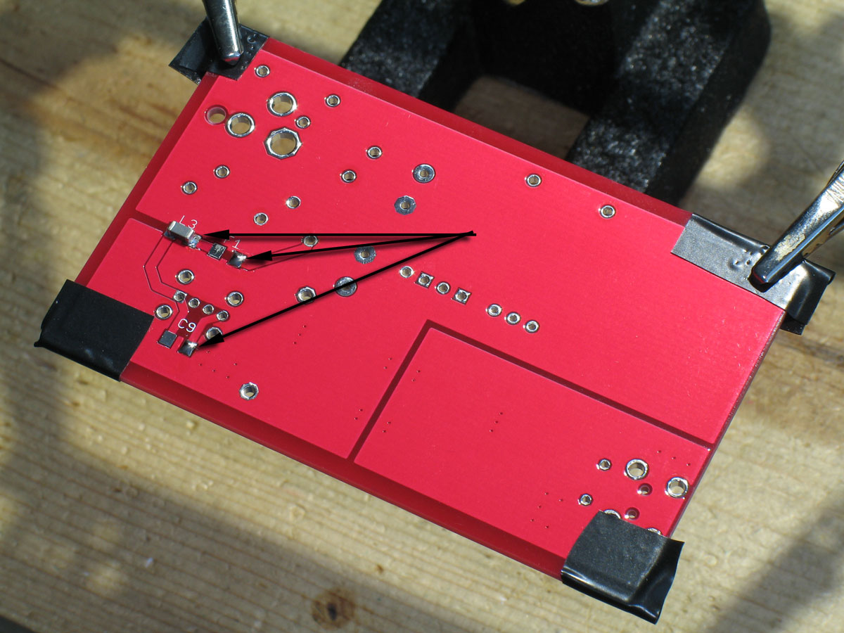
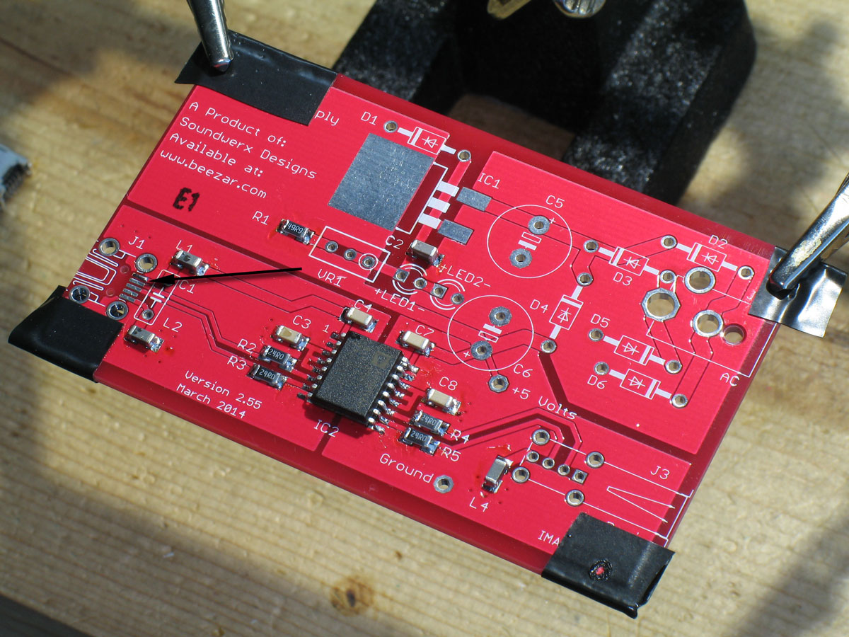
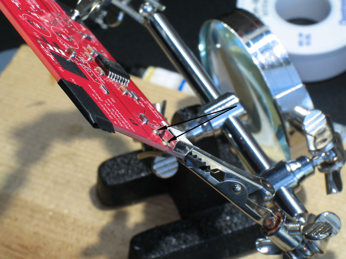
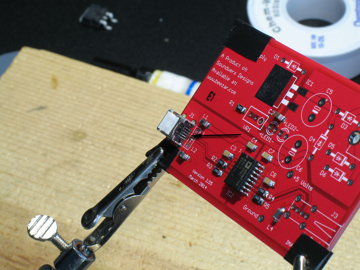
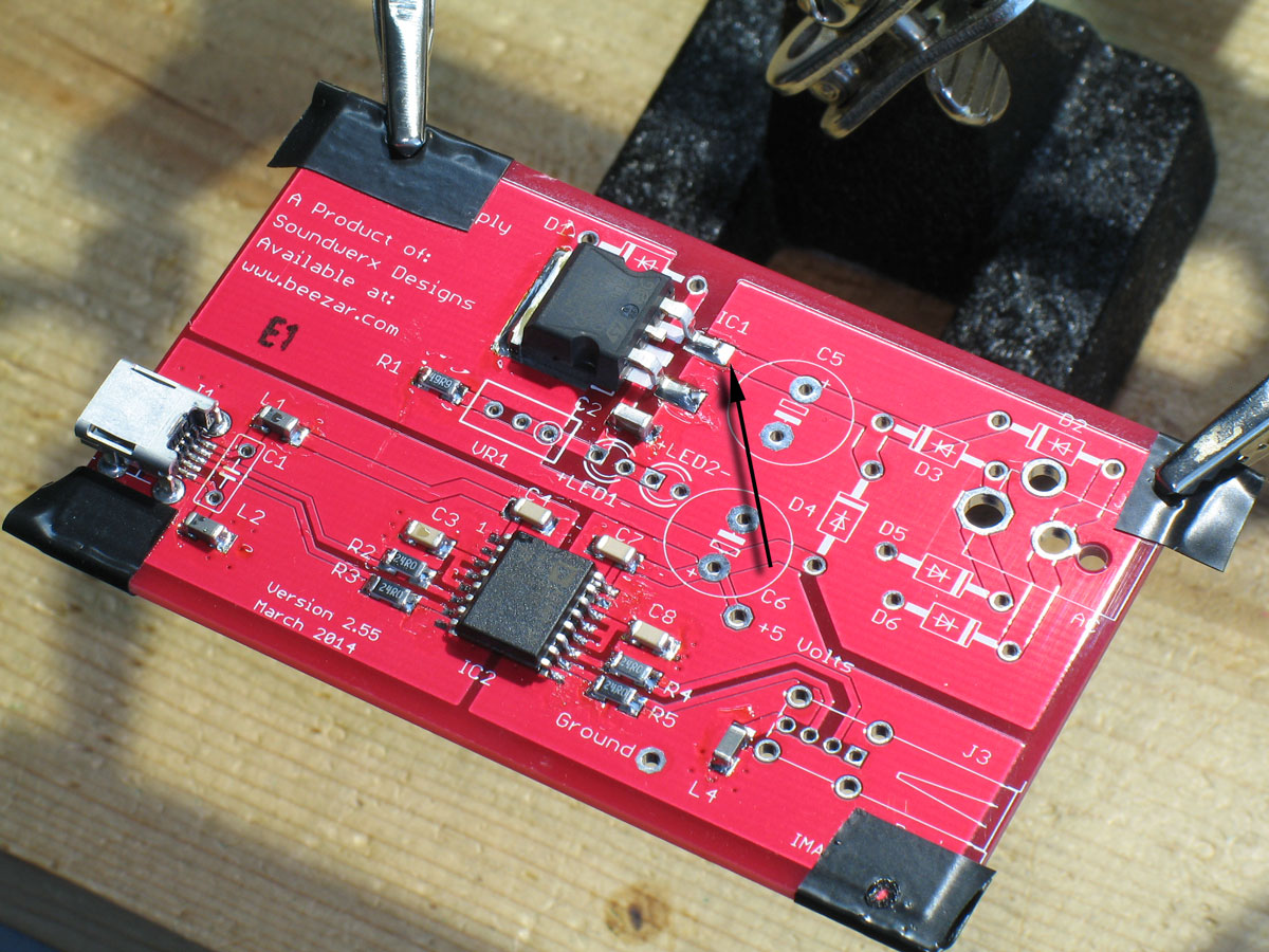
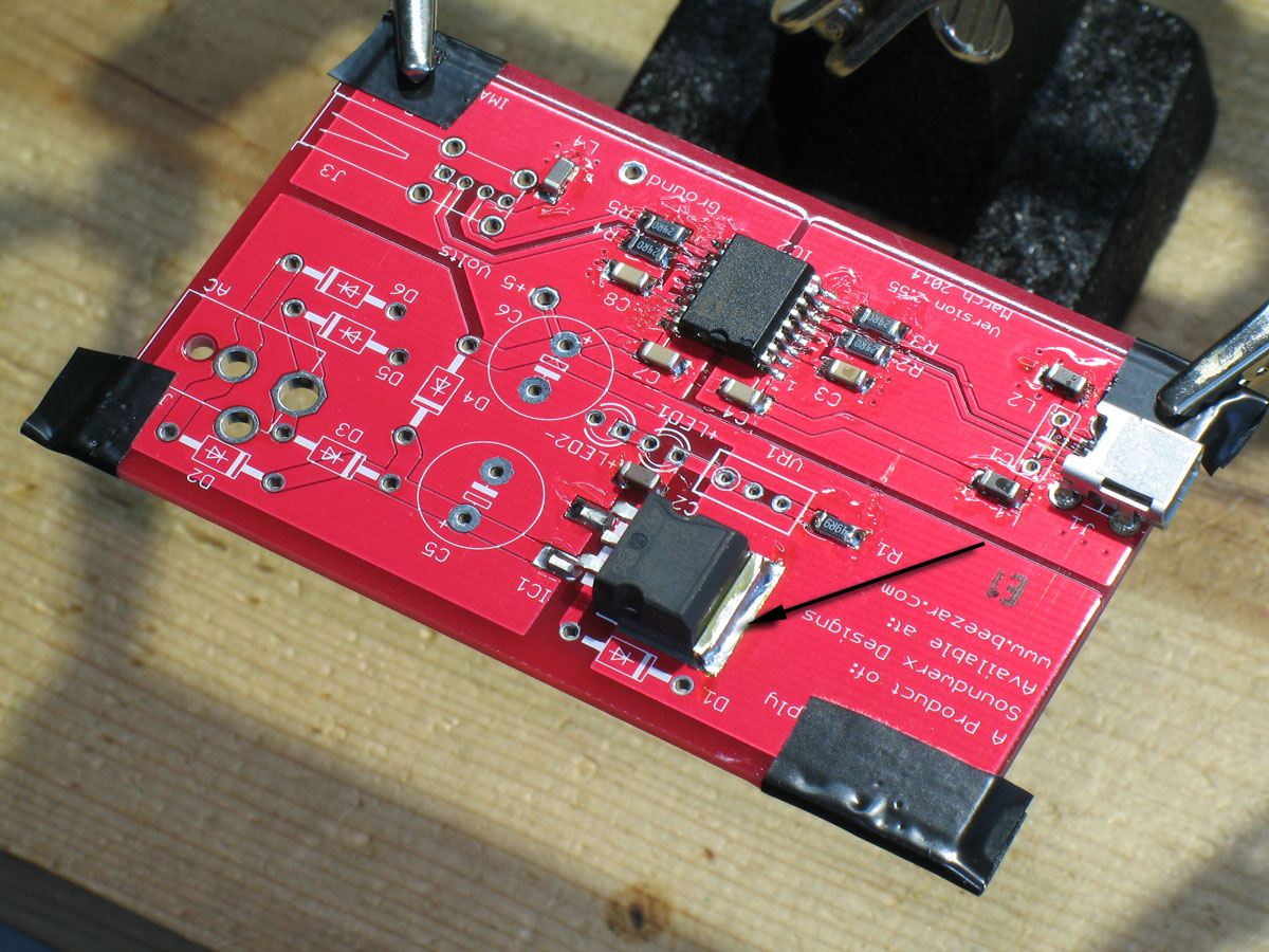
At this point, we want to flip the board over and solder the remaining 1206 SMD parts.  Not to be misleading about what constitutes an SMD part, there are actually two remaining on the top side of the PCB. One is the mini-USB jack and IC1, the voltage regulator. Each of these require a little different technique than normal. In the case of the mini-USB jack, the connecting pins are SMD. In fact, they are smaller/closer-together than any other SMD part on the DoodleBug. That's OK, though, because they're still large enough to allow individual soldering - if you're careful. The method I came up with for the SMD mini-USB jack was to solder one of the pins, first - preferrably the top pin as shown in the pic below. That's because while the SMD mini-USB jack has both metal and plastic locating pins, none of them are anywhere near a press fit. If you start with those first, it's easy to move the jack out of alignment and it would be very difficult to fix. On the other hand, soldering an "anchor" pin from the jack's electrical connection pins means that the jack is pretty much aligned with everything. Here we see the pad tinned for that specific purpose: Here we see my stubby fingers holding the SMD mini-USB jack in place while soldering the pin we tinned above. You can do this because the soldered pin is not in contact with any of the metal that forms the frame of the jack. So, you shouldn't get burned. To finish the mini-USB jack, thoroughly solder the frame side tabs and then complete the soldering for the rest of the pin connections. The jack may undergo quite a bit of stress and torquing over time, so it's important to get good structural joints with all of the solder filling the PCB holes around the frame tabs. This pic gives a side view and shows how your solder should wick up from underneath the PCB (where the solder joint is made) to the top surface and some distance up the side of the mini-USB jack frame. This will ensure that the jack doesn't come loose from the PCB or that it doesn't rip out some traces if something torques a connected cable loose: Here we see J1, the mini-USB jack, soldered in place. Note the SMD pins are soldered to the pads (arrow): Next up is IC1, the SMD version of an LM317 voltage regulator. The same SMD soldering principles apply. Tin one pad (indicated by the arrow). Then place the iron on the pad to re-melt the solder, while moving the chip into place using tweezers with the left hand. Note that because of the size of the part, it may take more solder to fully tin the pad and solder the other pad. Here we've flipped the PCB around so that you can get a good look at the soldered tab. This will be similar to soldering heat sink pins, if you've ever done that. The tab and the plated ground plane underneath will "sink" a lot of heat. So, solder one area at a time by adding solder, smoothing and moving a bit further until you get a joint all across the tab. Keep in mind that the LM317 is very robust, but you can fry it if you hit it with enough heat! If you paid attention and referenced this with the Step-by-Step section, you may notice that my sequence is not in agreement here. That's because in doing the photos while building, I chose to finish all the SMD parts first. However, it turns out the through-hole diodes have less height above the PCB than IC1 (I figured that out after the fact.). So, it's probably best to follow the Step-by-Step sequence if you're particular about soldering all the shortest parts, first. |